Difference between revisions of "Hardware"
Dark samus (talk | contribs) |
Dark samus (talk | contribs) |
||
| Line 159: | Line 159: | ||
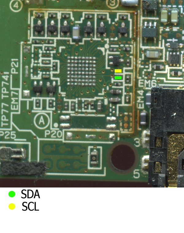
This is the interface for the 'NEW' WiFi module (based on Atheros AR6002) first included in DSi. | This is the interface for the 'NEW' WiFi module (based on Atheros AR6002) first included in DSi. | ||
| − | The proprietary | + | The proprietary DS-mode WiFi is colored yellow, pins are unknown. |
I²C eeprom is colored blue: | I²C eeprom is colored blue: | ||
Revision as of 08:45, 1 January 2017
This page lists and describes the hardware found inside the Nintendo 3DS. Many of these parts are custom made and are expanded upon here or in other pages.
Common hardware
| Type | Description |
|---|---|
| ARM11 Processor Core | Old3DS: ARM11 2x MPCore & 2x VFPv2 Co-Processor 268MHz(~268111855.956 Hz).
New3DS: 4x MPCore, 4x VFPv2, able to run up to 804MHz (see below). It also has an optional 2MB L2 cache. |
| ARM9 Processor Core | ARM946 134MHz(~134055927.861 Hz), |
| GPU | DMP PICA 268MHz, |
| VRAM | 6 MB within SoC. |
| Top screen | 800x240, with only 400 usable pixels per eye per line. |
| Bottom screen | 320x240, with resistive touch overlay. |
| DSP | CEVA TeakLite. 134Mhz. 24ch 32728Hz sampling rates. |
New3DS exclusives are able to clock the CPU at 804MHz, but this appears to be limited to the currently running application/app cores. Timed by running svcGetSystemTick on either side of a long idle loop to stay in the current process context. svcGetSystemTick uses a tick counter running at 268MHz in this mode.
On New3DS: when Home Menu is active, the system runs at 804MHz. For everything else, it's 268MHz, except when the app(let) has the required flag set. See here and here for details, regarding clock-rate and cache.
For New3DS-only there are multiple clock-rate multiplier values available in hardware, but since the relevant code is only implemented in the New3DS ARM11-kernel, the only non-normal clock-rate available with official kernel code is 3x.
Specifications
| Type | 3DS | 3DSXL | 2DS | N3DS | N3DSXL |
|---|---|---|---|---|---|
| SoC | CPU CTR (1048 0H)
CPU CTR (1214 32) |
CPU CTR A (1226 60)
CPU CTR (1037 21) |
CPU CTR B (??) | CPU LGR A (1444 86) | CPU LGR A (1446 17) |
| FCRAM | 2x64MB Fujitsu MB82M8080-07L | Fujitsu MB82DBS16641 | Fujitsu MB82DBS1664 | ?? | Fujitsu MB82MK9A9A |
| Top Screen | 3.53 in, 3D | 4.88 in, 3D | 3.53 in(?) cropped from a single panel | 3.88 in, 3D | 4.88 in, 3D |
| Bottom Screen | 3.00 in | 4.18 in | 3.00 in(?) cropped from a single panel | 3.33 in | 4.18 in |
| Storage | Toshiba THGBM2G3P1FBAI8 1GB | Samsung KLM4G1YEQC 4GB (in 1.3GiB SLC mode)
Toshiba THGBMBG4P1KBAIT 2GB (MLC, approx. 1.8GiB usable) | |||
| Audio Codec | TI PAIC3010B 0AA37DW | ?? | ?? | TI AIC3010B 39C4ETW | TI AIC3010D 48C01JW |
| Gyroscope | Invensense ITG-3270 MEMS Gyroscope | ?? | ?? | ?? | ?? |
| Accelerometer | ST Micro 2048 33DH X1MAQ Accelerometer Model LIS331DH | ?? | ?? | ?? | ?? |
| Wifi | Atheros AR6014 | ?? | ?? | ?? | Atheros AR6014G-AL1C |
| Infrared IC | NXP S750 0803 TSD031C | ?? | ?? | ?? | NXP S750 1603 TSD438C |
| Custom Microcontroller | Renesas UC CTR | ?? | Renesas UC CTR 324KM47 KG10 | Renesas UC KTR | Renesas UC KTR 442KM13 TK14 |
| PMIC? | TI 93045A4 OAAH86W | ?? | ?? | TI 93045A4 38A6TYW G2 | TI 93045A4 49AF3NW G2 |
- [11] Official Documentation
- [5],[10] According to iFixit.com (source):
- Datasheet for memory is for a chip in the same series, it has less memory than the one inside the 3DS (128mbits vs 512mbits).
- There is a trove of data on the FCC website at [1].
- [12] This IC is somewhat similar to this.
FCRAM
There is one FCRAM (Fast Cycle RAM) IC in the 3DS, produced by Fujitsu and branded as MB82M8080-07L. The Fujitsu MB82M8080-07L chip internally contains 2 dies, where each die is branded MB81EDS516545 and MB82DBS08645.
The MB81EDS516545 die is a CMOS Fast Cycle Random Access Memory (FCRAM) with Low Power Double Data Rate (LPDDR) SDRAM Interface containing 512MBit storage accessible in a 64-bit format. The MB81EDS516545 is suited for consumer applications requiring high data bandwidth with low power consumption.
SoC
The 3DS has much of it's internals housed in a SoC (System on Chip) just like it's predecessors. This is done to reduce build costs, cut down on power consumption, as well as make the PCB layout less complex and make the system harder to tamper with. The SoC, branded as the Nintendo 1048 0H, contains the CPU, GPU, DSP and VRAM.
According to official documents, the CPU used is a dual-core ARM11 CPU, clocked at 268MHz. One core is dedicated to system software, while the other is used for application programming, each known as the syscore and appcore, respectively.
GPU
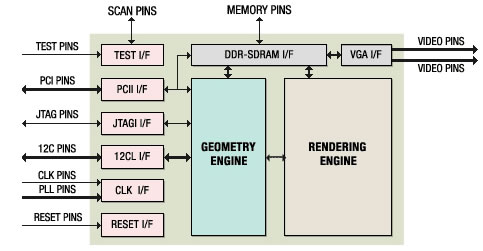
Designed by Digital Media Professionals Inc. (DMP) and codenamed PICA200, 268Mhz.
Block diagram of an ULTRAY2000 based architecture PICA200:
PICA200 is compatible with OpenGL ES 1.1. It furthermore provides unique functionality for:
- Per-fragment lighting ("Lighting Maestro")
- Hard- and soft-shadowing ("Shadow Maestro")
- Polygon subdivision ("Figure Maestro")
- Bump mapping and procedural textures ("Mapping Maestro")
- Rendering of gaseous objects ("Particle Maestro")
Some parts of the extended functionality are provided in hardware by an extended geometry pipeline. Most importantly, PICA200 has three programmable vertex processors. There is furthermore a unit called Primitive Engine, which is a geometry shader unit (using the same instruction set as vertex shaders) with support for variable-size primitives. The Primitive Engine functionality may be disabled, and the geometry shader unit then acts as a fourth vertex processor. See Shader_Instruction_Set for more information on the shader instruction set.
Fragment lighting is implemented as an optional pipeline step during pixel processing. It's implemented by having the vertex shader output an additional attribute describing the transformation (represented by a quaternion) to surface-local space. This per-vertex quaternion can then be interpolated across screen space to calculate dot products relevant for lighting (e.g. light vector dot normal vector). To provide support for advanced lighting models, these dot products are used as indices into programmable lookup tables. With this setup, PICA200 in particular supports the shading models Blinn-Phong, Cook-Terrance, Ward, and microfacet-based BRDF-models.
PICA200 supports four texture units, the fourth of which is used exclusively for procedural texture generation.
SDIO controller
Nintendo recommends SD cards up to 32 GB however the internal SDIO controller seems to support SD cards up to 2.19 Terabyte (32-bit sector number). It's unknown if it really can handle that much. 128 GB was tested and works fine however it causes a major slowdown of the system especially at boot.
Images
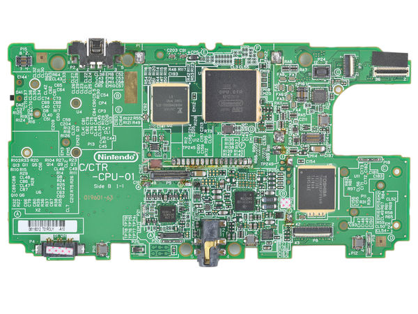
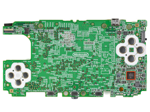
Front
Back
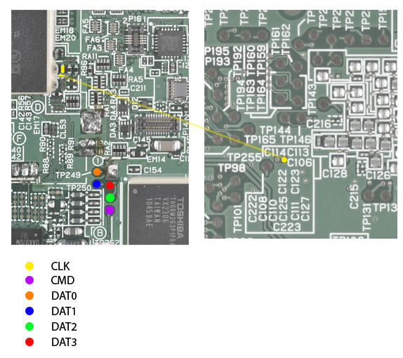
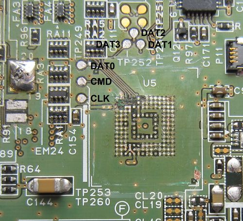
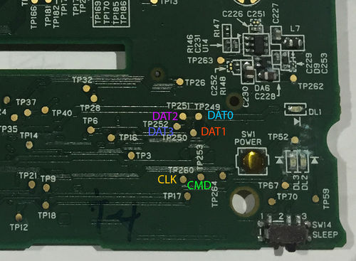
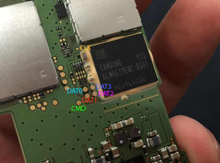
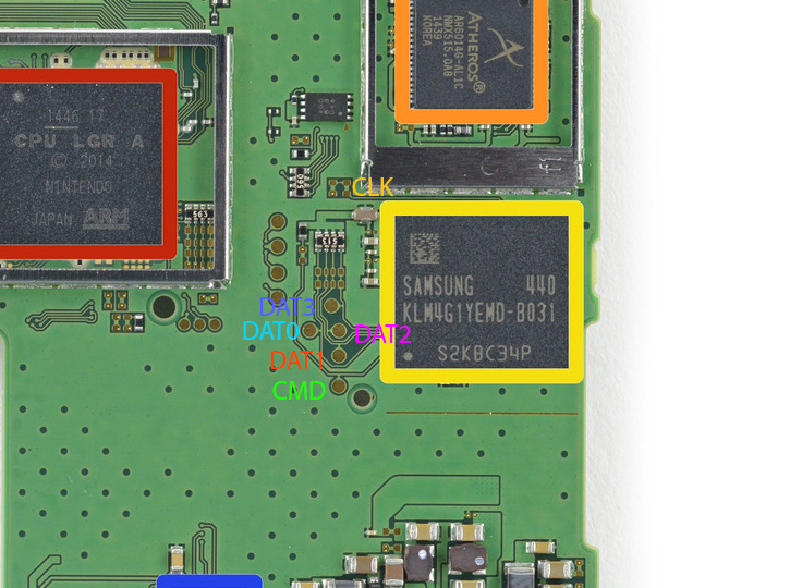
NAND pinout
NAND dumping has been successful, but the image is encrypted.
Normal model
XL model
2DS
New 3DS
New 3DS XL
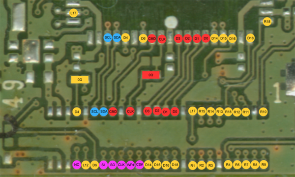
WiFi dongle pinout
SDIO interface is colored red:
- CLK
- CMD
- D0, D1, D2, D3
This is the interface for the 'NEW' WiFi module (based on Atheros AR6002) first included in DSi.
The proprietary DS-mode WiFi is colored yellow, pins are unknown.
I²C eeprom is colored blue:
- SCL
- SDA
SPI Flash is colored purple:
- CLK
- CS#
- SI
- SO
- WP#
- NC
Auxiliary Microcontroller (MCU)
Monitors HOME button, WiFi switch, 3D slider, volume control slider. Controls LEDs, various power supplies via an I²C connection to the PMIC.
Two I²C buses are attached to the MCU. For one, the SoC is the master; for the other, the MCU is the master.
Devices attached to MCU master I²C bus:
- MCU (master)
- Fuel Gauge
- Accelerometer (slave address 0x18)
- PMIC
- maybe more?
Devices attached the the SoC master I²C bus:
- SoC (master)
- MCU
- LCD
- Camera
- QTM (New3DS-only)
The MCU uses the RL78 ISA.
The MCU uses some custom Special Function Registers, but documentation for much of the hardware protocol/general SFRs can be found here.
