Difference between revisions of "Hardware"
m |
m |
||
| Line 8: | Line 8: | ||
| SoC || Nintendo 1048 0H (Custom): CPU, GPU, VRAM & DSP all on one chip. || N/A || N/A | | SoC || Nintendo 1048 0H (Custom): CPU, GPU, VRAM & DSP all on one chip. || N/A || N/A | ||
|- | |- | ||
| − | | Processor Core || ARM11 MPCore 2x | + | | Processor Core || ARM11 MPCore 2x 268MHz & 2x VFP Co-Processor || [http://infocenter.arm.com/help/index.jsp?topic=/com.arm.doc.ddi0360f/index.html] || [11] |
|- | |- | ||
| GPU || [http://en.wikipedia.org/wiki/PICA200 DMP PICA] 268MHz || N/A || [11] | | GPU || [http://en.wikipedia.org/wiki/PICA200 DMP PICA] 268MHz || N/A || [11] | ||
Revision as of 18:56, 3 November 2011
Specifications
| Type | Name | Datasheet | Source |
|---|---|---|---|
| SoC | Nintendo 1048 0H (Custom): CPU, GPU, VRAM & DSP all on one chip. | N/A | N/A |
| Processor Core | ARM11 MPCore 2x 268MHz & 2x VFP Co-Processor | [1] | [11] |
| GPU | DMP PICA 268MHz | N/A | [11] |
| DSP | 134Mhz. 24ch 32728Hz sampling rates. | N/A | [11] |
| VRAM | 6 MB within SoC. Independent of system memory (FCRAM). | N/A | [11] |
| FCRAM | 2x64MB Fujitsu MB82M8080-07L | [2][3][4] | [5] |
| Storage | Toshiba THGBM2G3P1FBAI8 1GB NAND Flash | N/A | N/A |
| Power Management | Texas Instruments PAIC3010B 0AA37DW | N/A | FCC filing |
| Gyroscope | Invensense ITG-3270 MEMS Gyroscope | [5] | N/A |
| Accelerometer | ST Micro 2048 33DH X1MAQ Accelerometer Model LIS331DH | [6] | N/A |
| Wifi | 802.11b/g Atheros AR6014 | [7] | N/A |
| Infrared IC | NXP infrared IC, "S750 0803 TSD031C" | N/A | [10] |
| Auxiliary Microcontroller | UC CTR, custom Nintendo microcontroller | N/A | N/A |
- [11] Official Documentation
- [5],[10] According to iFixit.com (source):
- Datasheet for memory is for a chip in the same series, it has less memory than the one inside the 3DS (128mbits vs 512mbits).
- There is a trove of data on the FCC website at [8].
FCRAM
There is one FCRAM(Fast Cycle RAM) in the 3DS.
DESCRIPTION
The Fujitsu MB82M8080-07L chip internally contains 2 dies, where each die is branded MB81EDS516545 and MB82DBS08645. The MB81EDS516545 die is a CMOS Fast Cycle Random Access Memory (FCRAM*) with Low Power Double Data Rate (LPDDR) SDRAM Interface containing 512MBit storage accessible in a 64-bit format. MB81EDS516545 is suited for consumer application requiring high data band width with low power consumption.
Images
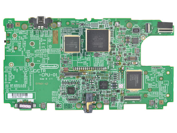
Front
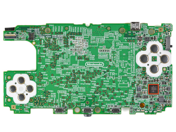
Back
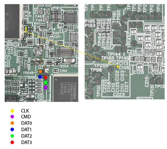
NAND pinout
NAND dumping has been successful, but the image is encrypted.
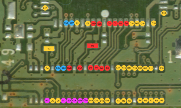
WiFi dongle pinout
SDIO interface is colored red:
- CLK
- CMD
- D0, D1, D2, D3
This is the interface for the 'NEW' WiFi module (based on Atheros AR6002) first included in DSi.
The proprietary and by now ancient DS-mode WiFi is colored yellow, pins are unknown.
I2C eeprom is colored blue:
- SCL
- SDA
SPI Flash is colored purple:
- CLK
- CS#
- SI
- SO
- WP#
- NC
Auxiliary Microntroller
Monitors HOME button, WiFi switch, 3D slider, volume control slider. Controls LEDs, various power supplies.
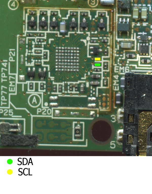
Devices attached to I2C bus:
- UC (master?)
- Accelerometer (slave address 0x18)
- SoC (master? slave?)
